
30Pcs / 15Pairs HIFI Female Headphone 2 Pin Audio Jack Plug Replace for DIY Focal Utopia Headset Cable Connector Silver Adapter |
33345.36

Новое поступление
Характеристики
*Текущая стоимость уже могла изменится. Что бы узнать актуальную цену и проверить наличие товара, нажмите "Добавить в корзину"
| Месяц | Минимальная цена | Макс. стоимость | Цена |
|---|---|---|---|
| Sep-18-2025 | 0.39 руб. | 0.23 руб. | 0 руб. |
| Aug-18-2025 | 0.16 руб. | 0.59 руб. | 0 руб. |
| Jul-18-2025 | 0.14 руб. | 0.75 руб. | 0 руб. |
| Jun-18-2025 | 0.54 руб. | 0.57 руб. | 0 руб. |
| May-18-2025 | 0.11 руб. | 0.84 руб. | 0 руб. |
| Apr-18-2025 | 0.89 руб. | 0.99 руб. | 0 руб. |
| Mar-18-2025 | 0.75 руб. | 0.49 руб. | 0 руб. |
| Feb-18-2025 | 0.24 руб. | 0.93 руб. | 0 руб. |
| Jan-18-2025 | 0.27 руб. | 0.59 руб. | 0 руб. |
Описание товара


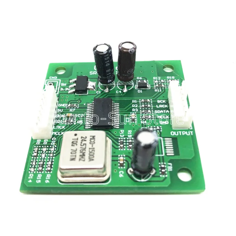
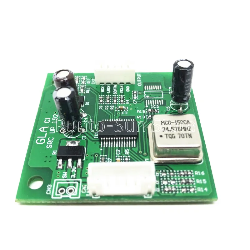
I2S frequency-up 192K/24BIT board for improving the decoding effect of DAC
Using the best SRC4192 chip at present, IS2 input is asynchronously raised to 192K sampling rate, 24-bit data output, and the highest sampling rate is 212 kHz.
Dynamic range: 144 dB (- 60 dBFS input,BW = 20Hz to FS/2, A weighting)
THD + N:-140 dB (0 dBFS relative input, BW = 20Hz to FS/2)
Through resistance change, I/O format support: I2S, left alignment, right alignment, TDM mode
Default input format - - - I2S
Default output format - I2S 192khz/24bit
Matters needing attention:
1. This board is only suitable for CMOS level input, not TTL level input. The simple judgment method is to measure the output signal foot voltage with a multimeter when it is not connected to this board. If it is about 1.6 volts, it will be suitable. Otherwise, it will not be able to use about 2.5V. Otherwise, it will burn the chip and burn the chip wrongly.
2. DAC using this product must support 192K/24-bit decoding, otherwise it can not be used. If you do not understand, please refer to the chip manual.
3. There is a certain risk in refitting. Only with the electronic foundation can we start. Our shop is not responsible for any damage during the refitting process.
Interface Description:
CN1 INPUT signal input socket signal description, marked on board
GND - ----- Grounding
5V - - - Connect 5V power supply, must supply 5V to 12V voltage to work normally.
BCK - ----- Bit Clock Input
SDI - ----- SDATA Data Input
LRCK - ----- left and right clock input
MCLK - --- Main clock input (this foot can not be connected)
Explanation of CN2 OUTPUT Signal Output Socket
BCK - ----- Bit Clock Output
LRCK - --------- left and right clock output
SDATA--Data Output
MCLK - ----- Main Clock Output
GND - ----- Grounding
Annex notes:
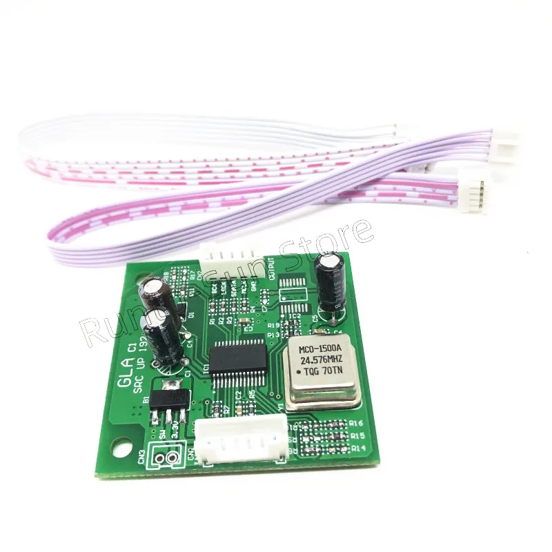
Equipped with input and output wiring


Смотрите так же другие товары:


